I am a Graphics Hardware Engineer in the Image Processing Unit at Intel India, working on Graphics Architectures and Physical design optimization from synthesis to GDSII. I have been a aprt of some really interesting projects here so far. Currently, I am working on a new algorithm to solve cell congestion hotspots in a design by suggesting alternate locations considering timing slack and DRCs.
On the side of fun, I like to cook for friends & family. Ever so often, I also like to write poems at YourQuote. Like every music wannabe, I bought a keyboard recently and am sluggishly learning to play it. On weekends, I can be found in a quiet corner at some literary event in Bangalore.
I graduated from IIT Roorkee in 2018, where I was advised by Dr. Anand Bulusu. During my time at IIT Roorkee, I also had the pleasure to work with Dr. Sanjeev Manhas. For my hobby projects, I worked on some interesting stuff at the Artificial Intelligence & Electronics Section, IEEE Student Branch, and Mobile Development Group at IIT Roorkee.
During my bachelor’s, I had the opportunity to explore many fields, ranging from Analog circuits, CMOS Devices to delay modeling in digital circuits. I also got to work on Industry research problems during my Internship at STMicroelectronics with Mr. Pratap Narayan Singh and during my major thesis at IIT Roorkee.
I like interacting with my juniors. I did serve as a Teaching Assistant for the course ‘Semiconductor Devices’ twice and a mentor in the Institute’s Student mentorship program for freshmen undergrads.
Bachelor with Honors in Electronics and Communication, 2018
Indian Institute of Technology(IIT) Roorkee
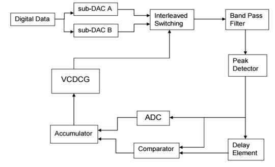
A feedback algorithm for removing timing mismatch problems and improving SNR of interleaved current steering DAC structures clocked at high frequency (in GHz) is proposed. The algorithm developed is tested to remove the timing errors at 4GHz frequency within a margin of 0.1% and improve the SNR by more than 24 dB and ENoB (Effective no. of bits) by more than 4 bits
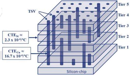
In this paper, we developed models to calculate the variation of threshold voltage and mobility due to stress around a TSV in 3D ICs. These models were then used to calculate delay variation of an inverter around a TSV.
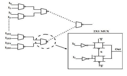
This paper presents a novel delay model for Inverter followed by Transmission Gate (Inv-Tx) structure. Our model is novel in the sense that it considers the series stack effect along with the internal node voltage and parasitic capacitances while treating the Inv-Tx structure as a single entity.